


 |
 |
 |
 |
 |
||||||||||||||
 |
 |
 |
||||||||||||||||
| updated on September 15, 2023 | |
| CLOISTER ROOM | |||
|
GE.I IMAGING AND NANOFABRICATION IN RESEARCH FOR ELECTRONICS RELATED COMPONENTS September 18 |
|||
| Chairs: Antonio D'ALESSANDRO, Sapienza University of Rome, Francesco BIANCARDI & Veronica SPARACINO, ZEISS | |||
Co-organized with: |
|||
|
The aim of the workshop is to highlight progress in research and technology related to microelectronics and novel structures where imaging and nanofabrication are indispensable methods steering the applications of these advanced devices. Over the workshop day, you can look forward to Latest technology insights from ZEISS, Kleindiek and Raith, Inspiring user presentations, a Get-together after the workshop for your networking. |
| 10:45 - 11:00 | Registration | |||||||
| 11:00 - 11:30 | Antonio D'ALESSANDRO, Director of CNIS, Sapienza University of Rome Giulio LA MEDICA, ZEISS Vittorio MORANDI - CV, Coordinator of the PNRR-RI project iENTRANCE@ENL, CNR Welcome |
 |
 |
 |
 |
|||
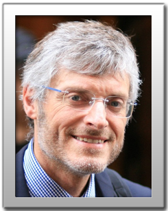
| 11:30 - 12:00 | Kirill ATLASOV ZEISS Microscopy Crossbeam-laser and Gemini imaging for semiconductor materials |
 |
|
|||||
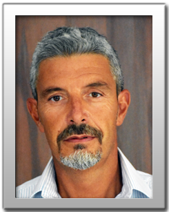
| 12:00 - 12:30 | Pasqualantonio PINGUE NEST, Pisa Lithography and characterization of nanostructures by scanning electron microscopy based techniques |
 |
|
|||||
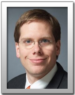
| 12:30 - 13:00 | Andrew SMITH Kleindiek The Prober Shuttle - a dedicated platform for performing nanoprobing tasks at low beam voltages addressing recent, current, and future technology nodes |
 |
|
|||||
| 13:00 - 14:00 light lunch | ||||||||
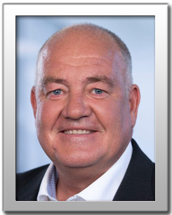
| 14:00 - 14:30 | Frank NOUVERTNE Raith GmbH Applications of Advanced Nanofabrication Utilizing Electron, Ion and Laser Beams |
 |
|
|||||
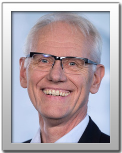
| 14:30 - 14:45 | Andreas REMSCHEID Raith GmbH Raith tools for nanofabrication |
 |
|
|||||
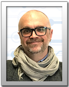
| 14:45 - 15:15 | Damiano GIUBERTONI FBK, Trento Multispecies FIB patterning: from nanometric prototypes to single defects in solids |
 |
|
|||||
| 15:15 - 15:45 break | ||||||||
| 15:45 - 16:15 | Annamaria GERARDINO CNR-IFN, Rome Electron Beam Lithography: A Versatile Tool for Research and Industrial Applications |
 |
|
|||||
| 16:15 - 16:45 | Filippo ROMANATO University of Padua, Padua Design and nanofabrication techniques for micro-lenses |
 |
|
|||||
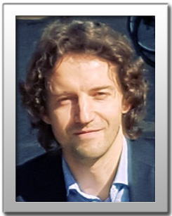
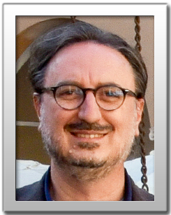
| 16:45 - 17:15 | Giorgio DIVITINI - CV IIT, Genoa Investigating the local properties of optoelectronic devices using Electron Microscopy and related techniques |
 |
|
|||||
| 17:15 - 18:00 | Open discussion and Closing remarks | |||||||
| 18:00 | Get together (drinks and fingerfood) | |||||||
| Back to Masterplan | |